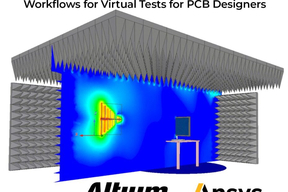
At LEAP Australia, we work closely with many customers who use Altium for their PCB designs and who have been incredibly excited by the recently announced collaboration between Altium & Ansys. This recently launched “SmartBridge” provides users with a bi-directional workflow between Altium ECAD and Ansys best-in-class simulation tools.
If you’re not familiar with Ansys, it offers broad multiphysics simulation capabilities which are most commonly used by PCB designers for:
- EMI/EMC and environmental testing
- PCB simulations to determine Signal Integrity, Power Integrity and EMI
- New ESD virtual testing according to IEC 61000-4-4
- Electronics environmental tests – Thermal, Shock, Vibration – to satisfy MIL-810G, DO-160G, GMW3172 standards
In April 2024, Thomas from LEAP’s Electronics Team was invited to speak at Altium Designer 24 launch event in Sydney. Today’s blog offers a series of highlights from that presentation – you can view the full playlist here – starting from his perspective on industry trends, then moving on the recently announced Altium-Ansys Smart Bridge (including a live demonstration), followed by a discussion of typical simulation examples including PCB analysis (power integrity, signal integrity, DCIR, electromagnetic interference / compliance, electrostatic discharge testing, and PCB environment tests).
Electromagnetics Industry Trends:
Especially in Australia, simulation is something we need to get out in into the broader industry. Simulation is critical to our global competitiveness as it allows our companies to increase product quality and reliability in a cost-effective way.
LEAP’s electromagnetics team specialises in helping customers to build effective workflows for typical issues in PCB design such as EMI/EMC. For example, we can simulate your PCB soldering processes and look into the detail of what the solder does and the quantitative impact of stresses and strains on PCB reliability.
Virtual testing is a strong trend worldwide. This applies not just to PCB design, but across all physics – consider magnetics designs, electronics cooling, electromagnetic compatibility shielding and much more. Ansys has a very strong Power Electronics workflow – we are able to merge highly dynamic power electronic semiconductors with parasitics – from a cable, from a package, and even from a full Altium board. So combining these details from Altium, together with component details and the parasitics in your circuit, you can generate have a very accurate physics-based model that can be utilised for many kinds of virtual testing.
In Australia, communication systems are of course also a hot topic – RF co-site interference, RAS, especially for defence applications, antenna design, antenna arrays and antenna mounting onto towers or other platforms.
Historical ECAD links to Simulation, how this changes with new Altium-Ansys Smart Bridge
In 2024, the best thing about this emerging partnership between Altium and Ansys is that now if you have designed your PCB in Altium, you’ve pretty much done more than 50% of your virtual prototype already – so in no time we can get it ready for simulation in Ansys, helping give you immediate feedback to improve board quality and overall product reliability.
There are many things to consider – mechanical topics, thermal topics, plus the classical electromagnetics topics. One more specialised topic includes modelling moisture absorption in different materials, so if your PCB is placed in a package and shipped (sometimes for a long durations, eg. 6 weeks) we can help predict if there is likely to be warping or deformation during transit.
Historically, we have used ODB++ and XML files to bring ECAD data into Ansys. However, this required extra work from the user regularly go into their BOM and create an XML file based on the reference designators and the values of your components. If you then import your ODB++ file plus the XML file, then all the components are in place. More recently, we’ve had the introduction of the EDB file which encapsulates pretty much all the information we need: the layers, the stackup, the materials, and also the components – so one file fits everything and goes directly from your Altium project into Ansys.
But even with these improvements from using an EDB file, some challenges remain – for example, if you do a couple of design iterations and make changes prompted by insights from your simulations, of course you must be careful to report & document everything correctly. In many cases, your updated designs can easily get lost in emails or may not be clearly documented with revision numbers. Typically, we see that this makes for a cumbersome and disorganised process, which has prompted this collaboration between Altium and Ansys with an aim to fix these issues.
The new Smart Bridge is enabled via your Altium 365 workspace to move files from Altium Designer seamlessly into Ansys. If you then make changes in Ansys, at the push of a button you can push those designs back into your Altium workspace (and your entire team can immediately begin working with the updated design in Altium designer). Our belief is that this supports a superior way of manifesting simulation results for your Altium PCB Designs, especially for multi-person teams, and certainly helps with Version Control as designs evolve during typical product development cycles.
In the video demonstration above (Part 2 of the presentation, embedded in this blog) for a Wi-Fi Bluetooth antenna, you can see how this all works in practice. There’s basically two buttons really – it’s just push and pull! You click on push and then you are able to move your data over to Ansys.
PCB Analysis Types: PI, SI, DCIR, EMI, EMC
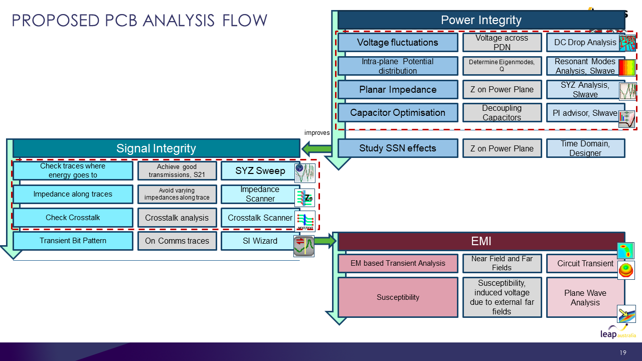
So what can you now achieve using this workflow? To get started, most Altium customers come to us wanting to do basic PCB simulations. We start with a plan to identify the root of any problems and then we work on Power Integrity. Once we have Power Integrity fixed, then Signal Integrity will be easier to consider, followed by Voltage fluctuations and DCIR, avoiding current crowding and hotpots in the power, so that then our PCB thermal design is manageable.
Watch the video above to understand how to simulate for:
- Power Integrity
- Eigenmode analysis
- Signal Integrity
- DCIR
- DDR5 compliance
- EMI nearfield and farfield analysis
- CISPR25 radiated/conducted emissions
As shown below, our recommended workflow shows how you can use your Altium data to make sure your PCB is pre-compliant before a prototype goes into any testing chamber:

ESD Virtual Testing:
For many years we have had the capability to conduct ESD testing using Altium data – we’ve used the circuit directly connected to PCB data. The test shown in the video below is a contact discharge: two switches, one is opening to charge the capacitor and the other one is opening to unleash the discharge of the capacitor of the energy to the board. The board is directly in 3D connected and this workflow can be used to test different grounding scenarios.
This ESD workflow and solver technology combines nonlinear air chemistry with electromagnetics, meaning we can also do air charge or discharge type of ESD tests. The tool understands the probability in each element if there is a breakdown and then changes the conductivity of that element to a very high value – so that current flow occurs. The workflow works very well with Altium PCB designs – you simply specify the region (for nonlinear air chemistry) and the round tip will then help to distribute the arc. This is a transient simulation and you can interactively move the tip over your PCB in different directions and at different locations to see what’s going to happen. During post processing, we usually look at E Fields but also look at the voltage that is coupled into the trace (by terminating the traces with a 50 Ohm resistor or similar).
PCB Environmental Testing:
In Australia, we know that many customers in mining and defence must carefully consider the ability for their PCBs to survive complex environmental testing before being released. Historically, people will build a physical prototype, put it into a test trial – conducting thermal tests, natural frequency, harmonic & random frequency, mechanical shock, etc.. You can view the full list in the video, which shows how much time and expense that it will take to go through all of these different tests for each board. Then, if you find that your board is failing, what do you do? You must design a new board and arrange a new physical prototype, then undertake this entire rigorous testing process again!
LEAP’s proposal as outlined in this Part 5 video above is to embrace simulation early – not after the prototype has been completed, but earlier at the part selection stage. At this point, it is cheap and effective to use simulation to properly and thoroughly understand the reliability of your board (and understand the impact of many variables).
Previously, this process was not embraced early enough, because the mechanical designer on your team probably considers FEA modelling of a full PCB to be very complicated and detailed – they must consider the leads, bonds, solder balls, coating and potting, plus you must input all the different material properties. So, historically, to a FEA engineer it seems like an absolute nightmare to attempt to simulate all these details in a PCB!
But that problem has been resolved with this new Smart Bridge. A second challenge was, once you have an accurate FEA result, how do I actually interpret these stresses and strains from my simulation – what does it really tell me in terms of how long it will survive in the field? You need a tool to convert those stresses and strains into meaningful data so that you know what your life curve is, and the probability of failure (using the appropriate standards). Now, we also have a solution for that, an example of which is shown in the video above.
It’s no longer a requirement to buy an expensive shaker table, you can evaluate your Altium PCB design in just a couple of hours using virtual testing!
Summary & how to get started with new Altium-Ansys workflow
As described in the video above, our wishes from many years ago have come true! The Altium-Ansys partnership provides the seamless link and interaction between design and simulation that our customers have been asking for. Engineers and designers can easily test and make changes, then pass the design back to the team. This workflow now provides the virtual PCB testbench which you’ve been waiting for – the time is now to get started! Contact LEAP to speak with an expert today.

